Inspection and measuring equipment market for OLED mobile device is expected to reach US$6.63 billion from 2017 to 2021

As the panel problem of mobile devices has become a hassle for consumers, each panel maker is strengthening the relevant inspection and measurement activities.


Inspection and measurement can contribute not only to enhance the quality and performance of products but also to enhance the brand image through customer satisfaction. In addition, it is expected that productivity and yield can be improved by stabilizing the process since it is possible to check the normal state of products at each process in real time.


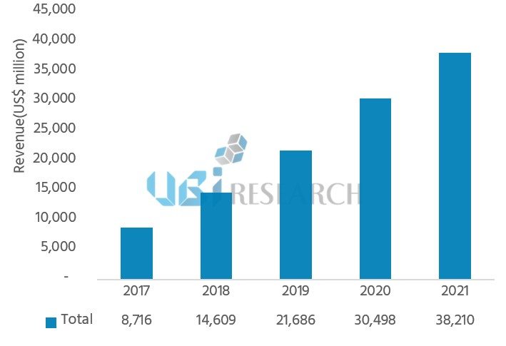
According to the ‘2017 Inspection and Measuring Equipment Report for OLED Mobile Device’ published by UBI Research, the inspection & measuring equipment market will reach a total of US$ 6.63 billion (about Korean Won 7.3 trillion) in the entire OLED equipment market from 2017 to 2021. In 2018, the investment for OLED inspection & measuring equipment is expected to be about US$ 1.45 billion (about KRW 1.6 trillion), with projected investment of US$ 1.6 billion (about KRW 1.8 trillion).


Choong Hoon Yi president of UBi Research announced that Samsung Display is currently in process of investment in A5 Gen6 flexible OLED line. LG Display is also reported to make a large-scale investment to raise OLED sales portion and Chinese OLED panel makers such as BOE and CSOT are making an active investment in OLED line. Hence, expectantly there will be constant market demand for inspection and measuring equipment.


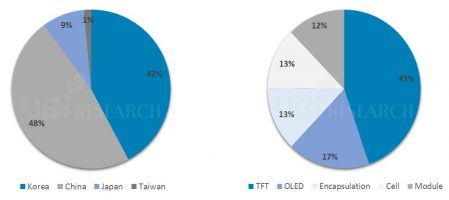
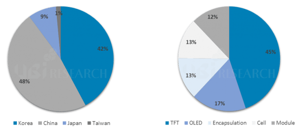
In the report, the inspection and measuring equipment market from 2017 to 2021 is classified from various viewpoints. According to this report, the equipment used for substrate and TFT process will account for the biggest market share of 50.6% of the total inspection and measuring equipment market from 2017 to 2021. Market share of cell inspection equipment is projected as 29.7%, OLED pixel as 12.7%, and encapsulation as 7%, respectively.  In the equipment market classified by test items, the equipment used for pattern inspection will account for 33.1% of the total market. Market share of repair equipment is projected as 21.3%, and light on/off inspection equipment as 16.4%, respectively.


Lastly, AOI equipment and laser repair equipment, the important piece of inspection and measuring equipment, are expected to reach US$ 2.33 billion and US$ 1.41 billion, respectively, from 2017 to 2021.

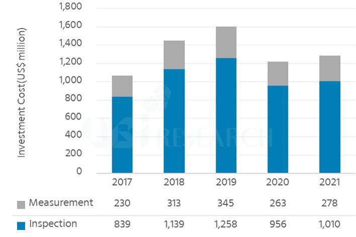
<Market forecast of inspection & measuring equipment for OLED mobile device from 2017 to 2021>


2017년부터 2021년까지 OLED Mobile 기기용 검사 · 측정장비 시장 66.3억 달러 기대

Mobile 기기의 panel 문제로 인해 소비자들의 불편이 가중되면서, 최근 각 panel 업체들은 검사 · 측정을 강화하고 있다.


검사 · 측정은 제품의 품질과 성능 향상뿐만 아니라 고객 만족을 통한 브랜드 이미지 제고에 기여할 수 있다. 또한, 각 공정에서 제품의 정상 유무를 실시간으로 점검할 수 있어 공정 안정화를 통한 생산성, 수율 향상이 가능할 것으로 예상된다.


유비산업리서치가 발간한 ‘2017 Inspection and Measuring Equipment Report for OLED Mobile Device’에 따르면, OLED 전체 장비 시장 중 검사 · 측정장비 시장은 2017년부터 2021년까지 총 66.3억 달러(약 7.3조원) 규모가 될 것으로 전망하고 있다. 2018년에는 14.5억 달러(약 1.6조원)의 OLED 검사 · 측정장비 투자가 진행 될 것으로 예상하고 있으며, 2019년에는 16억 달러(약 1.8조원)의 가장 많은 투자가 진행 될 것으로 전망하고 있다.


이충훈 대표이사는 Samsung Display는 A5 Gen6 flexible OLED line 투자를 진행중이며 LG Display는 OLED 매출 비중을 끌어올리기 위한 대규모 투자 내용 발표, BOE와 CSOT 등 중국의 OLED panel 업체들도 OLED 라인 투자를 적극적으로 진행하고 있기에 검사 · 측정장비는 지속적으로 수요가 있을 것으로 예상하고 있다.


본 보고서에서는 2017년부터 2021년까지의 검사 · 측정장비 시장을 다양한 관점에서 분류하여 전망하였다. 본 보고서에 따르면, 기판과 TFT에 사용되는 장비는 2017년부터 2021년까지 50.6%로 가장 큰 시장 점유율을 보이고 Cell은 29.7%, OLED 화소는 12.7%, encapsulation은 7% 순으로 전망하였다. 검사 · 측정 항목으로 분류한 장비 시장은 패턴검사가 33.1%, repair 21.3%, 점등 16.4% 순으로 나타났다.


마지막으로 검사 · 측정장비의 핵심 장비인 AOI 장비와 laser repair 장비는 2017년부터 2021년까지 각각 23.3억 달러와 14.1억 달러의 시장을 형성할 것으로 전망하고 있다.

<2017~2021년 OLED mobile 기기용 검사 · 측정장비 시장 전망>

LG전자, ‘올레드 풀비전’으로 더 크고 선명하게 본다


<출처 : LG전자>

LG전자가 하반기 전략 프리미엄 스마트폰에 OLED를 탑재한다.

LG전자는 18:9 화면비의 올레드 디스플레이를 제품 전면부에 꽉 채운 ‘올레드 풀비전(OLED FullVision)’을 하반기 전략 프리미엄 스마트폰에 적용한다. 디스플레이 크기는 전작인 LG V20의 5.7인치 보다 더 커진 6인치 대화면이지만 베젤을 줄여 제품의 크기는 오히려 작아진다.

LG전자는 “세계 최고 프리미엄 TV로 인정받은 LG 올레드 TV에서 쌓아온 디스플레이 기술을 바탕으로 스마트폰에서도 차원이 다른 시각적 경험을 제공할 계획이다”며, “수년간 축적해 온 올레드 기술로 차기 전략 프리미엄 스마트폰의 차별화된 고품격 디자인을 완성했다”고 밝혔다.

LG 전자의 하반기 전략 프리미엄 스마트폰에는 하단부의 회로와 절연막들을 패널 뒤편으로 휘어넘긴 ‘베젤 벤딩(Bezel Bending)’ 기술을 적용되어, 하단 베젤을 전작인 V20대비 약 50%까지 줄였다. 또한, 디스플레이 겉면의 강화유리는 디자인의 일체감을 강조하기 위해 상하좌우 가장자리를 곡면으로 처리하고 후면으로 이어지도록 하였다.

올레드 풀비전은 QHD+(1,440X2,880) 해상도를 가지며 최적화된 화질 알고리즘을 적용해 사진과 인터넷 컬러 규격인 sRGB 기준 148%, 디지털 시네마 컬러 규격인 DCI-P3 기준 109% 등 색재현율을 갖췄다.

LG전자는 올레드 풀비전에 대해 명암비가 뛰어나 깊고 생생한 화면을 구현함과 동시에 빠른 응답속도로 인해 움직임이 많은 동영상이나 화면 전환이 빠른 게임을 할 때 잔상 없이 박진감 넘치는 화면을 제공할 것이라 설명했다.

LG전자는 “사용자들이 항상 지니고 다니는 스마트폰의 특성을 고려해 디스플레이의 내구성도 한 단계 높였다”고 언급했다.

LG전자는 “올레드 풀비전은 플라스틱 기판 위에 화소를 배치한 P-올레드(P-OLED)를 기반으로 하기 때문에 유리 기판 디스플레이 대비 충격에 강하다.”며, “전면 디스플레이 위에 코닝 社(Corning®)의 최신 강화유리 ‘고릴라 글라스 5(Gorilla® Glass 5)’를 장착했고, 유리가 깨졌을 때 유리가루가 흩어지는 것을 막아주는 비산 방지(Shatter-resistant) 기술도 적용됐다”고 덧붙였다.

이 외에도 LG전자는 “내구성 강화를 위해 하드웨어 및 소프트웨어 기술을 적용했다”고 말했다. 또한, “화소에 공기가 닿지 않게 보호막을 덧씌워 산화를 최소화한 봉지 기술(Encapsulation, 封止 技術), 주변보다 유독 많이 사용한 화소를 찾아내 전력 소모량을 줄여주는 화소 스캐닝 프로그램 등 축적된 LG의 올레드 기술을 탑재해 디스플레이에서 나타날 수 있는 번인(Burn-In) 현상을 최소화했다”고 설명했다.

LG전자 MC사업본부장 조준호 사장은 “LG 올레드 TV에서 검증된 세계 최고의 디스플레이 기술을 총 집약해 스마트폰의 품격 높은 디자인과 차원이 다른 화질을 제공할 것”이라고 강조했다.


LG Electronics, watching bigger and clearer on ‘OLED FullVision’

<Source: LG Electronics>


LG Electronics will have a strategic premium smartphone equipped with OLED in the 2nd half this year.

LG Electronics will apply OLED FullVision, an 18: 9 aspect-ratio OLED display completely filling the entire screen panel to a strategic premium smartphone in the 2nd half. The size of the display is 6inch wide- larger than 5.7 inches of the previous model LG V20, but the size of the product is rather smaller by reducing the size of the bezel.
Based on the display technology obtained from LG OLED TV, which has been recognized as the world’s best premium TV, LG Electronics plans to provide a different level of visual experience of smartphone; “With OLED technology which has been accumulated over the years, we have completed the differentiated high-class design of the subsequent strategic premium smartphone.”
In the LG Electronics’ strategic premium smartphone, the “bezel bending” technology has been embedded in, which makes the circuit and insulating layers at the bottom of the panel bent backwards and the lower bezel reduced by about 50% compared to the previous model V20. Toughened glass on the outer layer of display is curved all around edge and is smoothened along the contour line of the backside to emphasize a sense of unity on the design,

OLED FullVision has a QHD + (1,440×2,880) resolution and an optimized screen quality algorithm equipped with a color gamut of 148% based on sRGB, default color space for photography and internet, and 109% based on digital cinema color standard DCI-P3.

LG Electronics stated that OLED FullVision should present a deep and vibrant screen with excellent contrast ratio and fast response time will provide a full-fledged screen without afterimages for fast-moving video or games.

LG Electronics also said, “The durability of the display has been upgraded as well, considering the portability of smartphone. OLED Full Vision is stronger than glass substrate displays because it is based on P-OLEDs with pixels placed on plastic substrates,”; “Cutting edge technologies are embedded in such as Corning®’s latest tempered glass ‘Gorilla® Glass 5’ and shatter-resistant technology that prevents the glass powder from scattering when the glass breaks. ” LG added.

Additionally LG Electronics said, “We have applied hardware and software technology to enhance durability. Also encapsulation technology that minimizes oxidation by covering the pixels with a protective film to prevent air contact, and pixel scanning program that identifies heavily used pixels and reduces their power consumption. OLED technology has minimized the burn-in phenomenon that can occur on the display. ”

Joon-ho Cho, president of LG’s MC business director emphasized, “We will provide a high end smartphone with a different level of design and screen quality, integrating the world’s best display technologies proven by LG OLED TV.

UBI Research , Published the Market Report on OLED Manufacturing Equipment

■The OLED equipmentmarket is expected to reach $84.9 billion in 5 years.

■Korean and Chinese panel companies will take over 90% of investment in panel equipment.


According to ‘2017 OLED Manufacturing Equipment Annual Report’ published by UBI Research, the entire equipment market of OLED is expected to total$84.9 billion(about 93trillion KRW) from 2017 to 2021. In 2017, $16.4 billion(about 18 trillion KRW) will be invested in OLED equipment.

The OLED equipment for the market analysis is largely categorized by process into 5 kinds of equipment; TFT, OLED, encapsulation, cell, and module. The investment costs including distribution equipment and test equipment of each process are calculated, and touch-related equipment is excluded from the market analysis.

Hyun Jun Jang, a senior researcher of UBI Research forecasts that the two countries will lead the OLED market due to the massive investment from both Korean panel companies occupying the OLED industry and latecomers Chinese panel companies.

According to this report, China and Korea will actively invest in OLED equipment from 2017 to 2017, showinga 48% and a 42% OLED market share, respectively. In particular, the two countries are expected to make the largest investment of $32.8 billion(about 36 trillion KRW) in 2017 and 2018.

Samsung Display has been expanding small and medium OLED lines to be applied to Galaxy series and Apple, and LG Display has been investing in both small & medium and large-size OLED lines. China’s BOE and CSOT are likely to invest heavily in OLED line because especially BOE has decided to invest more than 30K in small and medium OLED lines every year since 2017.


<left) OLED Equipment Market Share by Process,    right) OLED Equipment Market Share by Country>


From 2017 to 2021, itis forecast that TFT equipment, OLED pixel patterning equipment, encapsulation equipment, cell equipment, and module equipment will have a 45%, 17%,13%,13%, and 12% market share, respectively. In near future, the demand for flexible OLED will be likely to increase so that cell and module equipment will gain more importance having a 25% market share.

[New OLED report] Market report on AMOLED Component and Material for mobile devices

UBI Research published AMOLED component and material report for mobile devices. The report forecasted the future market by selecting 16 key component and material among the various component and material required for producing rigid AMOLED and flexible AMOLED for mobile devices.

According to the report, first, it is classified that the glass required for producing AMOLED for mobile is for substrate, encapsulation and carrier which is supporting PI substrate for producing flexible AMOLED essentially and the market is expected to reach US$ 92 million in 2017. In 2021, it is expected to grow up to US$ 185 million which is 2 times more than current.


The report also forecasted about the cover window market attached to outermost of AMOLED through a detailed analysis. The cover window market is expected not only for the 2D cover window for rigid AMOLED and the 3D cover window for flexible AMOLED currently used but for the plastic cover window market which is essential for a foldable smart phone in the future.

The cover window market of these 3 types is expected to grow rapidly with the growth of the flexible AMOLED market and to reach US$ 11.9 billion in 2021.


[신간 OLED 보고서] 모바일 기기용 AMOLED 부품소재 시장 보고서

AMOLED 부품소재 보고서 발간 보도자료.

유비리서치에서 모바일 기기용 AMOLED 부품소재 보고서를 출간하였다. 이 보고서는 모바일 기기용 rigid AMOLED와 flexible AMOLED를 생산하기 위해 필요한 각종 부품 소재들 중에서 핵심 부품소재 16종을 선별하여 향후 시장을 전망하였다.

<2017 모바일 기기용 OLED 부품소재 보고서, 유비리서치>

본 보고서에 따르면 우선 모바일 AMOLED 제조에 필요한 유리는 기판용과 encapsulation용, flexible AMOLED 제조에 필수적인 PI 기판을 지지할 carrier용으로 분류하였으며 2017년 시장은 92백만 달러로 예상하고 있다. 2021년에는 현재 보다 2배 성장한 1.85억 달러 시장으로 성장할 전망이다.

<2017 모바일 기기용 OLED 부품소재 보고서, 유비리서치>

또한 본 보고서에서는 AMOLED의 최외곽에 부착되는 커버 윈도우 시장에 대해서도 세밀하게 분석하여 전망하고 있다. 커버 윈도우 시장은 현재 rigid AMOLED에 사용되는 2D 커버 윈도우와 flexible AMOLED용 3D 커버 윈도우 시장을 비롯해서 향후 foldable 스마트 폰에 필수적인 플라스틱 커버 윈도우 시장도 전망하고 있다.

이들 3개 종류가 만드는 커버 윈도우 시장은 flexible AMOLED 시장 성장과 함께 급성장하여 2021년은 119억달러 규모가 될 전망이다.

<2017 모바일 기기용 OLED 부품소재 보고서, 유비리서치>


모바일 기기용 OLED 부품소재 시장 급팽창한다


<2017 모바일 기기용 OLED 부품소재 보고서, 유비리서치>

OLED를 제조하는데 필요한 부품과 소재는 기판을 포함하여 TFT, OLED, encapsulation, touch screen, cover window, drive IC 등이 있다.

삼성전자 스마트폰 Galaxy에 의해 주도되던 모바일 기기용 OLED 시장에 Apple과 중국 기업들이 동참함에 의해 삼성디스플레이를 비롯하여 중국 디스플레이 업체들의 Gen6 투자가 봇물 터지듯 증가하고 있다.

이에 따라 OLED 제조에 필수적인 부품소재 시장 역시 급팽창하고 있다.

유비리서치 조사에 의하면 2017년 모바일 기기용 OLED 부품소재 시장은 87.2억달러 규모이나 2021년에는 382억달러까지 급성장할 것으로 전망하고 있다.

국가별로 보면 한국의 부품소재 시장이 2017년 82.7억달러이며 94.9%의 시장을 점유하고 있으나, 2021년에는 중국의 부품소재 시장이 22.3%까지 증가하며 한국의 부품소재 시장은 72.2%로 낮아질 것으로 전망하고 있다.

<2017 모바일 기기용 OLED 부품소재 보고서, 유비리서치>


OLED Frontier Forum’s 3rd Section Panel Discussion Summary

The 3rd section of the 1st OLED Frontier Forum (Jan 28), OLED’s Future, held a panel discussion with government, industry, and academia experts discussing OLED industry development strategy, such as next generation technology development, convergent areas, and personnel training, and future forecast. OLEDNET summarized the answers that each expert gave to the questions of the panel chair (Professor Changhee Lee, Seoul National University).


Jun-hyung Souk (Professor, Sungkyunkwan University)

For SDC mobile, as the OLED depreciation is ending the OLED production cost is becoming almost the same as LCD. If OLED related experts stay within Korean industry as well as the technology, Korea can continue to lead for 4-5 years. In order to achieve the continued leadership, differentiation through flexible R2R has to be carried out, as well as the materials and encapsulation technology development.


Sung-Chul Kim (CTO, SDC)

As a-Si is an existing technology, there is no room for further advancement. Sharp’s difficulty in panel business is due to lack of technology research on the panel. Because one technology can only be used for approximately 7 months, diverse technology development is required.


In-byeong Kang (CTO, LGD)

Fast organizations cannot but win. Therefore, rapid change to OLED from LCD is needed. As difficult is the technology, cooperation between academia and industry is needed. Now is the time when this cooperation for next generation technology development is more in demand. LGD is putting in much effort for OLED profitability.


Sung-Jin Kim (Vice President, Toray Advanced Materials Korea)

Cooperation between materials and manufacturing equipment companies is important in solution process materials development. Particularly, how to control dry process is an important issue. Also, Kim expects the current solution process materials development to show tangible results in 3-5 years.


Junyeob Lee (Professor, Sungkyunkwan University)

Solution process is favorable for materials optimization. From the initial concentration on polymer materials, recently small molecule materials focused soluble materials development is being carried out, and how to implement common layer is an issue. Emitting layer is using the small molecule materials that are being used as evaporation materials. The difference is the higher cost as the solvent is used. Also, as there is an issue (formulation problem) when used in large area, solution is required.


Kyoung-Soo Kim (Vice President, Korea Display Industry Association)

Expert acquirement is a key issue. Through upgraded cooperation between industry and academia, and industries, cooperation between panel, manufacturing equipment, and materials has to progress into a positive cycle. Also the open platform regarding new OLED application is needed.


Young-Ho Park (PD, Korea Evaluation Institute of Industrial Technology)

Flexible display competitiveness acquirement is a big concern. Programs for challenging R&D, and high added value product/technology development, and R&D infra establishment (highly cost-effective R&D) have to be considered.


OLED Frontier Forum 제 3부 panel discussion 요약

제 1회 OLED Frontier Forum의 제 3부 ‘OLED 미래’에서는 정부, 업계, 학계 전문가들이 참석한 가운데, 차세대 기술개발, 융복합 분야, 인력양성 등 OLED 산업 발전 전략과 미래 전망에 대한 패널 토론이 진행되었다. OLEDnet에서는 사회자(이창희 교수, 서울대)의 질문에 대한 각 분야별 전문가들의 답변 내용을 요약하였다.


석준형 교수 (성균관대)

SDC Mobile의 경우 OLED의 감가상각이 끝나가기 때문에 OLED의 원가는 LCD와 거의 같아지고 있다. OLED관련 전문 인력만 빼앗기지 않으면 4~5년은 한국이 주도해나갈 수 있다.(Black Box화 전략) 지속적인 주도권 확보를 위해 flexible R2R로 차별화를 해야하며, 이와 더불어 소재와 encapsulation쪽 기술개발 필요하다.


김성철 CTO (SDC CTO)

a-Si는 기술적 차별성이 없다. Sharp의 panel 사업이 어려움을 겪은 이유는 panel에 대한 기술연구를 하지 않았기 때문이다. 한가지 기술로는 7개월 밖에 못 가기 때문에 다양한 기술에 대한 개발이 필요하다.


강인병 CTO (LGD CTO)

빠른 조직이 이길수 밖에 없다. 따라서 LCD에서 OLED로의 빠른 전환이 필요하다. 기술이 어려운만큼 산학연의 협력이 필요하며, 차세대 기술개발에 대한 산학연의 협력이 더욱 필요한 시점이다. LGD는 OLED 흑자를 위해 열심히 노력하고 있다.


김성진 전무(도레이 첨단 소재)

소재 업체와 장비 업체의 협력이 용액공정 재료 개발 시 중요하며 특히 Dry process를 어떻게 control을 할 것이냐가 중요한 이슈이다. 또한 현재의 용액공정 재료 개발은 3 ~ 5년 정도면 가시적인 결과를 볼 수 있으리라 판단한다.


이준엽 교수 (성균괸대)

용액공정이 재료 최적화에 유리하다. 초기 고분자 위주에서 최근에는 저분자 위주의 soluble 재료 개발이 이루어지고 있으며 공통층을 어떻게 가져가느냐에 대한 이슈가 있다. 발광층은 현재 증착 재료로 사용되고 있는 저분자 재료를 그대로 사용하고 있으며 차이점은 용매를 사용하기 때문에 가격 측면에서 현재는 비싸다는 이슈가 있으며, 또한 대형화 시 문제점(formulation 문제)이 있어 이에 대한 해결이 필요하다.


김경수 부회장(디스플레이 산업 협회)

전문인력 확보가 관건이며, 산학연 or 기업간 협력을 upgrade 시켜 panel-장비-소재간의 협력이선순환관계로 발전되어야 한다. 또한 새로운 OLED 응용분야에 대한 open platform이 필요하다.


박영호 PD(한국 산업기술평가 관리원)

Flexible 디스플레이 경쟁력 확보에 대한 고민이 크다. 도전적 R&D를 위한 program과 고부가가치의 상품/기술 개발, R&D infra 구축(가성비 높은 R&D)에 대해 깊은 고민을 해야 한다.

[Lighting Japan 2016] Yamagata University Develops Low Cost Flexible OLED Encapsulation

Innovation Center for Organic Electronics in Yamagata University in Japan discussed low cost flexible OLED encapsulation in Lighting Japan 2016 conference. Existing flexible OLED encapsulation mainly used hybrid encapsulation structure that forms multi-layer thin film passivation layers on top of OLED, and then applying adhesive organic material and laminating gas barrier film. The encapsulation structure presented by Yamagata University forms, of the hybrid encapsulation structure, thermoset resin and barrier film above OLED without multi-layer thin film passivation, and laminate at approximately 130 °C. Yamagata University announced that they were successful in transparent flexible OLED panel development on January 13 using encapsulation, and that this panel will be presented in Printable Electronics 2016 in Tokyo from January 27.


The OLED panel to be exhibited is a leaf shaped of 45 mm width, 110 mm length, weighs less than 1.2g, and 250 um thick transparent film substrate that can be folded.


According to Yamagata University, if the newly developed encapsulation is applied, the OLED lighting panel price can be reduced as passivation layer is not used. Also, Yamagata University revealed as it can satisfy both transparent and flexible categories simultaneously, it is estimated that it will become a key technology in future transparent flexible OLED lighting development.


Low Cost Flexible OLED Encapsulation, Yamagata University

Low Cost Flexible OLED Encapsulation, Yamagata University

[Lighting Japan 2016]야마가타 대학, 저비용 flexible OLED용 encapsulation 개발

일본 야마가타 대학에 있는 유기 전자 혁신 센터의 OLED 그룹은 Lighting Japan 2016의 conference에서 저비용 flexible OLED용 encapsulation에 대해 발표하였다. 기존 flexible OLED의 encapsulation은 OLED위에 한층 이상의 다층 박막 passivation layers를 형성한 후 adhesive organic material을 도포하고 gas barrier film을 laminating 하는 하이브리드 encapsulation 구조가 주로 사용되었었다. 이번에 야마가타 대학에서 발표한 encapsulation 구조는 하이브리드 encapsulation 구조에서 다층 박막 passivation 없이 thermoset resin과 barrier film을 OLED 위에 형성한 후 약 130도의 온도로 합착한다. 야마가타 대학은 encapsulation을 사용하여 지난 13일 ‘투명 플렉시블 OLED 패널’ 개발 및 프로토 타입에 성공했다고 발표 했으며, 이 패널은 27일부터 도쿄 빅사이트에서 열리는 ‘인쇄 전자 전시회 2016’에서 전시할 계획이라고 밝혔다.

전시될 OLED 패널은 폭 45mm, 길이 110mm의 나뭇잎 형태로 무게는 1.2g보다 가벼우며, 두께는 250um의 투명한 필름 기판으로 접을 수 있다.

야마가타 대학에 따르면, 새로 개발한 encapsulation을 적용하면 passivation layer를 사용하지 않아 OLED lighting panel의 가격을 낮출 수 있으며 투명과 플렉시블을 동시에 충족시킬 수 있기 떄문에 앞으로의 투명 플렉시블 OLED lighting 개발에 핵심 기술이 될 것으로 예상한다라고 밝혔다.

저비용 flexible OLED용 encapsulation, 야마가타 대학

[2015 OLED Evaluation Seminar] Professor Hong Mun-Pyo of Korea University Retraces Flexible OLED’s Key Issues

By Hyun Jun Jang


During the 2015 OLED Evaluation Seminar (December 4) hosted by UBI Research, Professor Hong Mun-Pyo of Korea University gave a talk titled Flexible AMOLED Gas Barrier Technology Development Status. Through this presentation, he discussed in detail flexible OLED’s outline, technological issues, and encapsulation among other key issues.


Flexible display signifies a display that was produced on top of flexible substrate, and not an existing glass substrate, which can bend, fold, or roll without breaking. Hong emphasized flexible display is the next generation display that can simultaneously satisfy consumers and panel makers, and an area that OLED can be more valuable compared to LCD.


There are 3 essential issues in flexible display, substrate, TFT array, and display processes, as well as ancillary issues such as application and cost. Hong reported key issues regarding substrate and display process.


Flexible display uses plastic substrate, instead of glass, that is strong against shock and can bend. Therefore, handling technology that manages plastic substrate is considered a key technology in flexible display production. Hong revealed that for handling technology, a film lamination method and vanish coating method are mainly used. A film lamination method is where plastic substrate is attached to carrier glass using adhesive before being processed and a vanish coating method is where the PI substrate is coated to the carrier glass before processing. He emphasized that no matter which method is used, the debonding technology used to detach the plastic substrate from the glass plays a crucial role in deciding yield.


Hong followed the substrate discussion with encapsulation technology. Encapsulation technology prevents moisture and oxygen that affect OLED panel’s performance from infiltrating in order to increase the display’s lifetime. As it is a core process that decides OLED panel’s yield, OLED panel production companies are focusing on optimum encapsulation technology development.


Key issues of encapsulation technology that is currently being applied to flexible OLED, barrier coating related issues are considered the most important. Barrier coating is the coating applied to the plastic substrate to overcome the limitations that occur as existing glass substrate is replaced by plastic. For flexible encapsulation, as can type or frit seal technologies that were used for glass encapsulation cannot be used, face seal or TFE technologies that can be applied to flexible are used. Also, as the permeability of oxygen and moisture has to be 10-6g/m2day or less, high performing barrier coating technology is needed.


When barrier coating is used to flexible OLED, generally 3 problems occur. Firstly, physically cracks or particles can develop. Regarding this, Hong explained that this issue can be solved if process is properly maintained. The second problem is micro defects that can arise on the surface of plastic film, which can be solved through optimized process, according to Hong. Lastly, nano-sized pin holes can come up. Hong revealed that multi-layers of barrier coating can solve this problem.


Generally, when OLED panel is produced the thickness of encapsulation layer is not a big issue. However, Hong emphasized that the thickness becomes a core issue when producing flexible OLED panel. He reported that hybrid structure of encapsulation where gas barrier cover plate is attached to passivation layer placed via PECVD can be the solution.


Although the most suitable process technology for hybrid encapsulation production is R2R, as appropriate results are not obtained when CVD is applied to R2R, Hong reported that research is being carried out toward the sputtering using direction. He revealed that if reflection plate is added to the sputtering equipment and neutron beam release is induced, defects that occur during the sputtering process can be reduced as the target thin film stabilizes.


홍문표 교수2

[2015 OLED 결산 세미나] 고려대학교 홍문표 교수, 플렉시블 OLED의 핵심이슈를 되짚다.

4일 유비산업리서치가 개최한 ‘2015 OLED 결산 세미나’에서 고려대학교 홍문표 교수는 ‘Flexible AMOLED용 Gas Barrier 기술개발 현황’이라는 제목의 강연을 통해 플렉시블 OLED의 개요와 기술적인 이슈, 플렉시블 OLED에 적용되는 encapsulation들에 대하여 심층적으로 이해하는 시간을 가졌다.

플렉시블 디스플레이는 기존의 평판 디스플레이의 특성을 그대로 유지하면서 기존 유기기판이 아닌 깨지지 않으며, 휘거나 구부리거나 말 수 있는 유연한 기판 위에 제작된 디스플레이를 의미한다. 홍 교수는 플렉시블 디스플레이는 소비자와 패널 maker를 동시에 만족시킬 수 있는 차세대 디스플레이라고 강조하며 OLED가 LCD보다 더 유용하게 적용할 수 있는 분야라고 밝혔다.

플렉시블 디스플레이에는 크게 기판과 TFT array 공정, 디스플레이 공정 이라는 3가지의 기술적인 이슈가 있으며 application과 cost 등 부수적인 이슈들이 있다. 이 날 홍 교수는 기판, 디스플레이 공정에 대한 핵심 기술에 대한 내용을 발표했다.

플렉시블 디스플레이에는 유리기판이 아닌 휘어질 수 있고 충격에 강한 플라스틱 기판을 사용한다. 그래서 플라스틱 기판을 다루는 handling 기술은 플렉시블 디스플레이 제작에 핵심적인 기술로 꼽힌다. 홍 교수는 “Handling 기술에는 adhesive를 사용해서 플라스틱 기판을 carrier glass에 붙이고 공정을 진행하는 film lamination 방식과 PI기판을 carrier glass에 코팅한 후 공정을 진행하는 vanish coating 방식이 주요하게 쓰인다.”고 밝히며 어떤 방식을 사용하던지 플라스틱 기판을 glass에서 떼내는 debonding 기술이 수율에 결정적인 역할을 한다고 강조했다.

홍 교수는 이어서 디스플레이 공정 중 encapsulation 기술에 관해 논했다. Encapsulation 기술은 디스플레이의 수명을 증가시키기 위해 OLED panel의 성능에 영향을 주는 수분과 산소의 투습을 방지하는 기술을 말하며 OLED panel의 수율을 결정짓는 핵심 공정이기 때문에 각 OLED panel 제조 업체는 최적의 encapsulation 기술을 찾는데 집중하고 있다.

현재 플렉시블 OLED에 적용되는 encapsulation의 핵심 이슈로는 barrier coating에 대한 것이 가장 중요하게 꼽힌다. Barrier coating은 기존 유리기판을 플라스틱으로 대체하면서 발생하는 한계를 극복하기 위해 플라스틱 기판에 부착하는 코팅을 말한다. 플렉시블 encapsulation에는 기존 glass encapsulation에 쓰이는 can type나 frit seal과 같은 기술이 사용될 수 없기 때문에 플렉시블에 적용 가능한 face seal이나 TFE과 같은 기술이 사용된다. 또한 투습되는 산소와 수분의 양은 10-6g/m2day이하가 되어야 하기 때문에 고성능의 barrier coating 기술이 필요하다.

플렉시블 OLED에 barrier coating이 사용될 때 일반적으로 3가지 문제가 발생한다. 먼저 물리적으로 크랙이나 파티클이 발생할 수 있다. 이와 관련하여 홍 교수는 공정 관리를 잘해주면 해결 가능하다고 밝혔다. 두번째로는 플라스틱 필름의 표면에 마이크로 단위 크기의 defect가 발생할 수 있다. 이에 대해서는 공정을 최적화해서 해결 가능하다고 밝혔다. 마지막으로 나노사이즈의 pin hole이 생기는 문제가 발생할 수 있는데 이에 대해서는 barrier coating을 다층박막으로 형성해 해결할 수 있다고 밝혔다.

홍 교수는 보통의 OLED 패널을 제작할 때는 encapsulation 층의 두께가 크게 이슈가 되지 않지만 플렉시블 OLED 패널을 제작할 때는 두께가 핵심적인 이슈가 된다고 강조하며 PECVD로 passivation 층을 올리고 그 위에 gas barrier cover plate를 합착하는 hybrid 구조의 encapsulation이 이에 대한 솔루션이 될 수 있다고 발표했다.

또한 Hybrid encapsulation 제조 시 가장 적합한 공정 기술은 R2R이지만 CVD를 R2R에 적용할 경우 적절한 특성이 나오지 않기 때문에 sputtering을 사용하는 방향으로 연구되고 있다고 하며, sputtering 장비에 반사판을 설치하여 중성화 빔이 방출하도록 유도하면 target 박막을 안정화시켜 기존 sputtering 공정 중에 발생되는 defect를 줄일 수 있다고 밝혔다.


[Expert Talk] Dr. Mauro Riva, SAES Group’s OLED/OLET Business Developer, on Encapsulation

Dr. Mauro Riva, SAES Group’s OLED/OLET business developer, discussed his views on OLED in general as well as SAES Group’s technology through his interview with the OLEDNET and presentation at the OLEDs World Summit (October 27-29) titled ‘The Encapsulation Question’.


Encapsulation is required to prevent the oxidation of emitting and electrode materials by blocking moisture and oxygen. It also protects the device from mechanical and physical shocks. The basic configurations of encapsulation can be divided into 3: glass-to-glass, barrier film lamination, and thin film encapsulation methods. Glass-to-glass configuration is applied to rigid AMOLED for mass produced mobile, barrier film lamination and thin film encapsulation methods are used for flexible AMOLED, and barrier film lamination is used for large area AMOLED panel for TV.


Source: SAES Group, OLEDs World Summit 2015

Source: SAES Group, OLEDs World Summit 2015


According to Dr. Riva OLED encapsulation is still facing the same issues it had since the beginning: OLED materials’ extreme sensitivity to oxidizing agents and moisture in particular. He added that OLED materials can also be very sensitive to heat or radiations, generating many process constraints. Encapsulation technology is directly related to the lifetime of the OLED device and Dr. Riva raised several questions regarding the current issues surrounding the technology including the appropriate target lifetime, best definition of “lifetime”, and reliability of the “accelerated tests”. He emphasized that while much progress have been made, a “single optimal, universal solution” does not exist yet to meet various encapsulation requirements depending on OLED architecture, materials, environment, applications, etc. As such, encapsulation materials have to be specifically engineered to meet different types of OLED devices while having “exceptionally high barrier properties, and active fillers or getters, capable of absorbing water on a single molecule basis”. Thus, perfecting this technology is a very challenging task, and, according to Dr. Riva, something that requires in depth collaboration between advance encapsulation materials providers and OLED makers.


For their part in this technology progression, Dr. Riva reported that SAES Group provides a very large portfolio of active edge sealants, active transparent fillers, and dispensable getters. He explained that the portfolio is the results of deep know-how in functional polymer composites (FPC), “specially tailored to address customers’ specific OLED designs and processes”. Discussing the FPC during his talk in OLEDs World Summit, Dr. Riva emphasized the versatility of this approach.


Source: SAES Group, OLEDs World Summit 2015

Source: SAES Group, OLEDs World Summit 2015


Regarding application methods for SAES Group’s FPC products, Dr. Riva explained that they can be dispensed via screen printing, blading, syringe, ink-jetting, ODF (one drop filling), and even be employed in thin film encapsulation structures, to make them simpler and more reliable. Furthermore, Dr. Riva reported that while SAES Group considers syringe dispensing as one of the main methods for applying their FPC, “ink-jetting is also becoming more and more widespread, together with ODF, especially for active fillers”.


Dr. Riva believes the FPC could play an important role in making the encapsulation more effective, and that SAES Group can “leverage on its advanced materials expertise” and in-depth getter/purification knowledge, to “perfect FPC based encapsulation solutions for OLEDs”. 11% of SAES Group’s net sales is allocated to Research and Innovation every year with strong cooperation with universities and R&D centers. The company is collaborating with many companies in diverse areas of interest such as OLED lighting, manufacturing equipment, specialized food packaging, and gas barrier films. This proactive and collaborating approach will enable the SAES Group to play a key role in developing more marketable OLED devices.


[인물탐방] SAES 그룹 OLED/OLET 사업부의 Encapsulation 파트 개발자, Mauro Riva 박사

SAES 그룹의 OLED/OLET 사업부의 개발자인 Mauro Riva 박사는 10월27일부터 29일까지 개최된 OLEDs World Summit에서 ‘The Encapsulation Question’라는 제목의 발표와 OLEDNET과의 인터뷰를 통해 OLED에 대한 자신의 관점과 SAES 그룹의 기술에 대해 논했다.

Encapsulation은 습기와 산소를 차단해 전극물질과 발광층의 산화를 막고 기계적, 물리적 충격에서 디바이스를 보호하기 위해 필요한 공정이다. 기본적인 encapsulation 배열 방법은 glass-to-glass와 barrier film lamination, thin film encapsulation 방법, 이렇게 3가지로 나누어진다. Glass-to-glass 배열 방법은 소형 모바일 양산에 쓰이는 rigid AMOLED에 적용되며 barrier film lamination과 thin film encapsulation 배열 방법은 플렉시블 AMOLED에 사용된다. 그리고 barrier film lamination은 TV에 쓰이는 대면적 AMOLED 패널에 사용된다.

oled summit

Source: SAES Group, OLEDs World Summit 2015

Riva 박사에 따르면 OLED 재료가 산화제와 습기에 대해 민감해서 발생하는 문제들은 OLED 등장부터 encapsulation이 발전한 현재까지도 아직 완전하게 해결되지 않았다. 그는 OLED 물질이 열과 방사선에도 매우 민감할 수 있기 때문에 공정에 대한 많은 제약을 만들어낸다고 덧붙였다. Encapsulation 기술은 OLED 디바이스의 수명과 직접적으로 연관이 있다. Riva 박사는 OLED 수명과 관련된 기술을 둘러싼 현재 이슈들에 대한 문제를 제기했다. 그는 “현재 encapsulation 기술은 많은 진보를 이루었다. 하지만 OLED 구조와 재료, 환경, 어플리케이션 등에 따라 다양한 encapsulation 솔루션이 요구되며 통합된 한가지의 솔루션은 존재하지 않는다.”고 강조했다. 이와 같이, encapsulation 재료는 요구되는 배리어 특성을 만족하면서도 OLED 디바이스의 각각 다른 유형을 충족하도록 설계되어야 한다. 그래서 이 기술을 완벽하게 적용하는 것은 매우 도전적인 과제며, Riva 박사에 따르면 encapsulation 재료 공급 업체와 OLED 패널 제작 업체 사이에 깊은 협력이 요구된다.

Encapsulation 기술 진보를 위한 SAES 그룹의 역할에 대해서 Riva 박사는 측면 sealant와 active transparent filler, dispensable getter에 대한 대규모 포트폴리오를 공급하고 있다고 발표했다. 그는 해당 포트폴리오는 “특정 고객들을 위한 특수 OLED 디자인과 공정”이라는 주제이며 기능성 고분자 화합물(FPC : Functional Polymer Composites)에 대한 깊은 노하우에 대한 결과라고 설명했다. Riva 박사는 OLEDs World Summit에서의 발표 중 FPC에 대해서 논하며 이 포트폴리오에 관해 “수많은 다양성을 내포하고 있다.”고 강조했다.

oled summit2

Source: SAES Group, OLEDs World Summit 2015

SAES 그룹의 FPC 제품들이 실제로 적용되는 방법과 관련해서 Riva 박사는 FPC 제품들은 screen printing과 blading, syringe, ink-jetting, ODF (one drop filling)으로 증착이 가능하다고 설명하며 특히 TFE 구조에 적용될 경우 더 간단하고 안정적으로 제작할 수 있다고 밝혔다. Riva 박사는 FPC가 encapsulation 공정을 좀 더 효과적으로 하는데 핵심적인 역할을 할 것으로 믿으며 SAES 그룹이 getter와 정제 기술, 첨단 소재에 대한 전문적인 지식을 바탕으로 FPC를 기반으로 하는 완벽한 OLED encapsulation 솔루션을 제공할 수 있다고 밝혔다. SAES 그룹는 매 년 순 매출액의 11%를 대학, 연구기관과의 협동 연구에 할당하고 있다. SAES 그룹은 현재 많은 업체와 협력을 하고 있으며 OLED 조명과 공정장비, 전문식품포장, gas barrier film 같은 다양한 분야에 관심을 기울이고 있다. SAES 그룹은 좀 더 시장성이 있는 OLED 디바이스를 개발하는데 핵심 역할을 담당하기 위해서 이런 선제적이고 협력적인 R&D를 주도하고 있다.

AIXTRON Supplies R&D Encapsulation Equipment OPTACAP

On 9 September, AIXTRON, a deposition equipment production company, revealed that they supplied encapsulation equipment OPTACAP to a major Asian display maker.


OPTACAP encapsulation is a research equipment that handles substrates size of 200mm x 200mm. AIXTRON revealed that this was ordered in the third quarter in 2015 and is scheduled to be delivered in the first quarter of 2016. The OPTACAP’s PECVD technology enables the deposition of barrier film used in TFE process of OLED display, OLED lighting, organic photovoltaic and flexible electronic device.


CTO (chief technology officer) of AIXTRON, Andreas Toennis, said, “thin-film encapsulation is an essential step within the OLED manufacturing process. Therefore, we are delighted to be able to provide an innovative solution to the industry which delivers excellent barrier films at high throughput. Therefore, this solution contributes to a significant reduction of manufacturing costs for the critical encapsulation process step within the production of flexible as well as rigid OLED devices”.


In April 2015, AIXTRON acquired PlasmaSi, located in Silicon Valley in order to develop OPTACAP encapsulation technology.

AIXTRON, R&D용 encapsulation 장비 OPTACAP 공급

증착장비 생산 기업인 AIXTRON은 9월 9일 OPTACAP라는 이름의 encapsulation 장비를 아시아 주요 디스플레이 생산 업체에 공급했다고 밝혔다.

OPTACAP encapsulation 장비는 200 mm x 200 mm size이며, R&D에 활용될 것으로 밝혔다. AIXTRON사는 “이 장비가 2015년 3분기에 주문되었으며 2016년 1분기에 출하될 예정이다. 또한  OPTACAP 장비의 PECVD 기술을 통해 OLED 디스플레이와 OLED 조명, 유기 광전지 등의 제조 공정 중 TFE에 사용되는 barrier film을 증착할 수 있다”라고 발표하였다.

AIXTRON SE.의 CTO(최고 기술 책임자)인 Andreas Toennis는 “TFE는 OLED 제조공정에서 필수적인 과정으로 AIXTRON는 고품질의 barrier film을 빠르게 형성하는 공정에 대한 솔루션을 개발하였다. 이 솔루션은 rigid OLED뿐만 아니라 flexible OLED의 핵심적인 공정인 encapsulation 과정에 들어가는 생산 단가를 크게 감소시켜줄 것으로 기대된다.“라고 말했다.

한편 OPTACAP encapsulation 기술을 개발하기 위해 AIXTRON은 2015년 4월, 실리콘밸리에 위치되어있는 회사인 Plasma Si를 인수한 바 있다.

Encapsulation Technology That Can Greatly Increase OLED Lifetime Unveiled

On July 29, at Chungcheong Display Forum held in Hoseo University in South Korea, an encapsulation technology that can greatly increase OLED lifetime was revealed.


Encapsulation technology prevents permeation of oxygen and moisture from affecting OLED panel’s performance and increases lifetime. As it is also the last process that decides OLED panel yield, OLED panel manufacturing companies are focused on finding the most optimal encapsulation technology.


The flexible OLED panel that is currently being mass produced uses hybrid structure of encapsulation where gas barrier cover plate is applied to the organic and inorganic stacks of passivation.


During this process, because cover plate with gas barrier characteristics is the key factor in deciding encapsulation performance the materials and technology are very important. The level of encapsulation that OLED panel requires is approximately 10-6g/m2day. The unit signifies the amount of permeation for 1m2 area a day. This amount is same as 1 drop of water in an area size of 6 World Cup stadiums.


Generally sputtering technology is used to form gas barrier layer. Sputtering technology is an evaporation technique where ions of the target material is coated to the substrate as noble gas, ionized via high voltage, collides against coating material.


This type of sputtering technology creates particles and defects during process. As such, in order to be applied to OLED, multilayer is required leading to a decrease in productivity and increase in production cost.


However, at the Chungcheong Display Forum, Professor MunPyo Hong of Korea University, revealed that defect that occurs during the existing sputtering process can be reduced by stabilizing target layer through installing reflector which induces neutral beam to be released.


According to Hong, this technology is sufficient to achieve the OLED level encapsulation standard of 10-6g/m2day even using a single layer. He revealed that this technology will be able to reduce the production cost and increase the productivity.


(a) Device Immediately After Production (b) Device with Insufficient Encapsulation with Insufficient Encapsulation (dark spot and pixel shrinkage occurs after certain amount of time) Source: UBI Research

OLED의 수명을 획기적으로 높일 수 있는 encapsulation 기술 공개

7월 29일 호서대에서 개최된 충청 디스플레이 포럼에서 OLED의 수명을 획기적으로 높일 수 있는 encapsulation 기술이 공개되었다.

Encapsulation 기술은 OLED panel의 성능에 영향을 주는 수분과 산소의 투습을 방지하여 수명을 증가시키는 기술이다. 또한 OLED panel의 수율을 결정짓는 마지막 공정이기 때문에 각 OLED panel 제조 업체는 최선의 encapsulation 기술을 찾는데 집중하고 있다.

현재 양산되고 있는 flexible OLED panel은 유무기 적층의 passivation에 gas barrier cover plate가 합착되는 hybrid 구조의 encapsulation이 적용되고 있다.

이 때 gas barrier 특성이 있는 cover plate가 encapsulation 성능을 결정짓는 핵심 요소이기 때문에 형성하는 재료와 기술이 매우 중요하다. OLED panel에서 요구되는 encapsulation의 수준은 10-6g/m2day이다. 이 단위의 의미는 1일에 1m2의 넓이에 투습되는 양을 의미한다. 이 정도의 양은 6개의 월드컵 경기장을 합친 크기의 공간에 한 방울의 물이 떨어지는 것과 같은 아주 작은 규모이다.

일반적으로 gas barrier layer를 형성하는 데에는 sputtering 기술이 사용되고 있다. Sputtering 기술은 고전압을 통해 이온화된 불활성기체가 코팅재료에 충돌하게 되고, 이 때 타깃물질의 이온이 튀어나와 기판에 달라붙어 코팅이 되는 증착기술이다.

이러한 sputtering 기술은 공정 중 particle이 발생하고 defect가 형성되기 때문에 OLED에 적용하기 위해서는 multilayer로 쌓아주어야 했다. 이 경우 생산성이 약화되고 원가가 증가되는 단점이 있었다.

하지만 충청 디스플레이 포럼에서 고려대학교 홍문표 교수는 sputtering 장비에 반사판을 설치하여 중성화 빔이 방출하도록 유도하면 target 박막을 안정화시켜 기존 sputtering 공정 중에 발생되는 defect를 줄일 수 있다고 발표하였다.

홍문표 교수에 따르면 이 기술은 single layer를 사용하면서도 OLED panel에서 요구하는 encapsulation의 수준인 10-6g/m2day를 달성하기 충분하기 때문에 원가를 낮추고 생산성을 높일 수 있다고 밝혔다.


A Place Where the Latest OLED Technology Trend Can Be Seen In One Glance UBI Research Hosts 2015 OLED Key Technology Seminar

A seminar where latest technology of next generation display, OLED (Organic Light Emitting Diode), can be easily understood will take place. UBI Research, a research company specializing in OLED (http://www.ubiresearch.co.kr, president: Dr. Choong Hoon Yii), revealed that it will hold 2015 OLED Key Technology Seminar in COEX (Samseong-dong, Gangnam-gu, Seoul, South Korea) on 27 Aug.

This seminar will discuss latest issues in OLED industry such as processes in flexible OLED, encapsulation, oxide-TFT, blue phosphorous emitting material, and solution process, and focus on technology development and its future.

Encapsulation, which decides OLED panel’s final yield and lifetime, is an important process that determines exterior design in flexible OLED and large size OLED panel. It is also sensitive to light characteristics in surface light structure. At the 2015 OLED Key Technology Seminar, Dr. Choong Hoon Yi (president of UBI Research) is scheduled to introduce, through process and material analysis, essential technology needed for OLED panel to continue its growth and encapsulation technology trends.

At this seminar, Dr. Nam Sung Cho of ETRI (Electronics and Telecommunications Research Institute) will give a presentation on display technology that utilizes white OLED technology that is receiving much interest by Korean display market. He will detail white OLED technology’s present and future from lighting to large size TV.

Professor Sung Kyu Park of Chung-Ang University, will introduce oxide material that is in spotlight as display and next generation wearable device. He will also talk about internationally much discussed related technology trends and future progress.

Further presentation topics by OLED top experts include:

– AMOLED panel technology trends analysis (Hyun Jun Jang, senior researcher of UBI Research)

– Oxide-TFT technology status (Professor Ga-Won Lee, Chungnam National University)

– Solution process and vacuum evaporation OLED material’s status and forecast (Professor Sung-Ho Jin, Pusan National University)

– High efficiency blue phosphorous emitting material development trend (Professor Jun Yeob Lee, Sungkyunkwan University)

– Flexible OLED technology trend

UBI Research holds OLED Key Technology Seminars every year from 2011 and provides place for networking and sharing of information. Seminar registration can be completed through UBI Research website (www.ubiresearch.co.kr).

프로그램2

[Update]최신 OLED 기술 동향을 한 자리에서 파악할 수 있는 세미나 장 열려… 유비산업리서치, ‘2015 OLED 핵심기술 세미나’ 개최

차세대 디스플레이로 자리매김한 유기발광다이오드(OLED)의 최신 기술 동향을 파악할수 있는 세미나 장이 마련된다.

‘OLED 전문 기업’ 유비산업리서치(http://www.ubiresearch.co.kr, 대표 이충훈)는 8월 27일(목) 서울 강남구 삼성동에 소재한 COEX에서 ‘2015 OLED 핵심 기술 세미나’를 개최한다고 밝혔다.

이번 세미나는 최신 OLED 산업에서 이슈 되고 있는 flexible OLED와 encapsulation(봉지기술), Oxide-TFT, 청색인광재료, solution process 공정 등에 대한 주제로 OLED 산업에서 주목할 만한 기술의 개발 현황과 전망에 대해 집중 소개한다.

OLED 패널에 있어서 최종 수율과 패널 수명을 결정하는 encapsulation은 Flexible OLED와 대면적 OLED 패널에서 외곽 디자인을 좌우하는 중요한 공정이며, 또한 전면 발광 구조에서는 광 특성에도 민감하게 작용한다. ‘2015 OLED 핵심 기술 세미나’에서는 유비산업리서치 이충훈 대표가 최근 OLED 주요 업체들이 사용하는 공정과 주요 재료들을 분석하여 향후 OLED 패널이 시장에서 지속 성장하기 위해 필수적으로 확보해야 할 기술과 encapsulation 기술 동향을 소개할 예정이다.

이 자리에서 한국전자통신연구원 조남성 박사는 최신 한국 디스플레이 시장에서 주목받고 있는 White OLED 기술을 기반으로 하는 디스플레이 기술에 대해 조명부터 대형 TV까지, 차세대 디스플레이의 핵심기술인 백색 OLED 기술의 현황과 미래에 대하여 설명한다.

아울러 중앙대학교 박성규 교수는 현재, 디스플레이 및 차세대 웨어러블 디바이스 소자로서 각광 받고 있는 산화물 전자소재의 특성 및 용액공정 기반으로 발전하고 있는 새로운 기술 및 응용에 대한 소개와 더불어 최근 국내외적으로 각광 받고 있는 관련 기술 동향 및 향후 발전 전망을 발표할 예정이다.

이 밖에도 ▲ AMOLED 패널 기술 동향 분석 (유비산업리서치, 장현준 선임연구원), ▲ 산화물박막트랜지스터 기술 현황 (충남대학교, 이가원 교수), ▲ 용액공정과 진공증착용 OLED 재료의 현황과 전망 (부산대학교, 진성호 교수), ▲ 고효율 청색 인광재료 개발 동향 (성균관대학교, 이준엽 교수), ▲ Flexible OLED 기술 동향, 이 OLED 최고 전문가들에 의해 다뤄진다.

유비산업리서치는 2011년부터 매년 OLED 핵심 기술 세미나를 개최 하며, OLED 전문기업으로서 OLED를 위한 가치 있는 공유의 장을 마련하고 있다. 세미나 참가신청은 유비산업리서치 홈페이지(www.ubiresearch.co.kr)를 통해 할 수 있다.


[Analyst Column] Encapsulation Technology, Where is it Going?

Yi Choong Hoon Yi, Chief Analysis / UBI Research

OLED market is heating up again. Rigid OLED market growth was temporarily stalled but with Samsung Electronics and LG Electronics’ new flexible (plastic) OLED products, Galaxy S6 Edge and G Flex 2 respectively, the smart phone market’s temperature is rising. In order to maintain the storm that iPhone brought, Apple is preparing to release smart watch equipped with LG Display’s plastic OLED. Additionally, LG Elec. is targeting the premium TV market with their 55 inch and 65 inch UHD OLED TV.

OLED panel leading company Samsung Display decided on Gen 6 line’s additional investment for flexible OLED production expansion. LG Display also decided on supplemental extension of Gen 4 line in Paju responding to the shortage of plastic OLED supply. Furthermore, JDI is joining in and expected to begin Gen 6 flexible OLED line establishment soon.

Recently announced Samsung Display’s decision to invest in large OLED line is the most encouraging news. Frontline leader in OLED display, Samsung Display mass produced 55 inch OLED panel using RGB OLED and LTPS TFT technology. However, halting the production, Samsung Display explored for technology with better business value and recently selected to produce large OLED panel using WRGB OLED technology.

OLED panel production technology can be largely separated into 3 parts: TFT, OLED, and encapsulation. Large OLED panel production technology is very difficult to obtain yield compared to small panel. Therefore, while the above 3 technologies are important in producing good panel, technology that can acquire good yield for mass production can guarantee business value. Particularly, as encapsulation is the last process, the final yield depends on the encapsulation method.

In that case, what encapsulation technology is most suitable for large area OLED panel production? As OLEDNET article published on January 12 mentions, from the technology trend perspective the answer is hybrid encapsulation technology. This technology is completed with device’s passivation film, moisture proof top plate that can cover the top, and organic material that adhere the top and passivation film. From the design trend perspective, the technology must be able to bend. Recently, the TV market is moving toward curved design, and to respond to rollable display as well the top plate has to be metal rather than glass. (Reference, 2015 OLED Encapsulation Report, UBI Research)

Hybrid encapsulation technology can be further divided into film method and dam & fill method depending on the adhesive structure between top plate and passivation film. Film method is being applied to mass production by LG Display, and dam & fill method was developed led by Sony. This method dispenses adhesive polymer liquid after organic dam installation on the panel border. This can only be used when the top plate is glass. LG Display completes the process by sealing the metal plate laminated with adhesive film to the device. A best suited technology for curved TV and rollable TV production.

The OLED panel for TV production technology decided by Samsung Display was initially known to select WRGB OLED structure similar to LG Display, but TFT and encapsulation technology have not yet been revealed. However, TFT technology is highly likely to be oxide TFT. (Reference February 27 OLEDNET article) LTPS TFT has high investment cost compared to oxide TFT and has low business value at similar performance.

What is left is encapsulation technology. For this technology also a method already commercialized by LG Display, film lamination method, is most suitable since metal plate is favorable for curved design. Metal plates is strong against external shocks and favorable for heat sink. Glass has lower heat conductivity compared to metal and requires additional protection against heat; this means that production cost can only increase. Considering design, protection against external shocks, and reduced heat sink cost, LG Display’s hybrid encapsulation technology that uses metal plate is the most ideal. Therefore, the direction that Samsung Display should also head toward is metal plate and film using method.

Although small OLED for mobile technology developed by Samsung Display became the norm, it is estimated that LG Display’s technology will become standard for large OLED panel production.

[Analyst Column] Encapsulation 기술, 어디로 가나?

이충훈, 유비산업리서치 수석 애널리스트


OLED 시장이 다시 달아 오르기 시작한다. Rigid OLED 시장 성장이 일시 제동이 걸려 있으나, 삼성전자와 LG전자는 flexible (plastic) OLED로 각각 Galaxy S6 Edge와 G Flex2를 내놓으면서 smart phone 시장에 다시 불을 지피고 있다. 또한 Apple은 iPhone 돌풍을 이어가기 위한 병기로 LG디스플레이가 생산하는 plastic OLED를 탑재한 smart watch를 출시 준비 중이다. 더불어 LG전자는 55인치와 65인치 UHD OLED TV로서 프리미엄 TV 시장 공략에 나섰다.

OLED 패널 생산 최대 기업인 삼성디스플레이는 flexible OLED 생산 확대를 위해 Gen6 라인 추가 투자를 결정하였으며, LG디스플레이 역시 plastic OLED 공급 부족에 대처하기 위해 파주에 Gen4 라인 보완 증설을 결정하였다. 여기에 JDI도 가세하여 Gen6 flexible OLED 라인 증설을 곧 추진할 예정이다.

가장 고무적인 것은 최근 언론에 공개된 삼성디스플레이의 대형 OLED 라인 투자 결정이다. OLED 산업을 최전방에서 리딩하고 있는 삼성디스플레이는 RGB OLED와 LTPS TFT 기술로서 55인치 OLED 패널을 양산하였으나 생산을 중단하고, 보다 사업성이 우수한 기술을 결정하기 위해 장고에 들어갔다, 최근에 WRGB OLED 기술로서 대형 OLED 패널을 생산하기로 결정하였다.

OLED 패널 제조 기술은 크게 3부분으로 나누어진다. TFT와 OLED, 마지막으로 encapsulation이다. 대형 OLED 패널 제조 기술은 소형 패널에 비해 수율 확보가 상대적으로 매우 어렵다. 따라서 상기 언급한 세가지 기술은 좋은 패널을 제작하기 위함도 중요하지만, 양산에서는 보다 양호한 수율을 확보 할 수 있는 기술이 사업성을 보장한다. 특히 encapsulation은 마지막 공정이기 때문에 최종 수율은 encapsulation 방식에 의해 결정된다.

그러면 대면적 OLED 패널 제조에 가장 적합한 encapsulation 기술은 무엇일까? 1월8일자 OLEDNET 기사에서 이미 언급한 바와 같이 기술 트랜드 관점에서 보면 hybrid encapsulation 기술이다. 소수의 passivation막과 상부를 덮을 수 있는 방습용 상부 기판, 그리고 상부 기판과 passivation막을 접착하는 유기재료로 이 기술은 완성된다. 디자인 트랜드 관점에서는 휘어질 수 있어야 한다. 최근 TV 시장이 curved 디자인으로 흐름이 바뀌고 있으며, rollable 디스플레이까지 대응하기 위해서는 상부 기판이 유리 보다는 금속이 필수적이다. (참조, 2015 OLED Encapsulation Report, UBI Research)

Hybrid encapsulation 기술에 사용되는 방식은 상부 기판과 passivation막을 접착하는 구조에 따라 다시 film 방식과 dam & fill 방식으로 분류된다. Film 방식은 LG디스플레이가 양산에 적용하고 있는 기술이며, dam & fill 방식은 Sony가 주도로 개발한 기술이다. 이 기술은 패널 외곽에 유기물로서 dam을 설치하고 접착성 고분자 액체를 도포하는 방식이다. 상부 기판이 유리일 경우에만 사용이 가능하다. LG디스플레이는 접착 필름이 라미네이션 된 금속판을 소자에 합착하여 공정을 완성한다. Curved TV와 rollable TV를 만들기에는 최적인 기술이다.

삼성디스플레이가 이번에 결정한 TV용 OLED 패널 제조 기술은 우선 LG디스플레이와 유사한 WRGB OLED 구조를 채택할 것으로 알려졌으나 TFT와 encapsulation 기술은 아직 공개되지 않았다. 그러나 TFT 기술은 역시 oxide TFT가 될 가능성이 높은 것으로 추정된다. (2월27일 OLEDNET 기사 참조) LTPS TFT는 oxide TFT와 비해 투자비가 높기 때문에 유사한 성능에서는 사업성이 매우 낮기 때문이다.

남은 것은 encapsulation 기술이다. 이 기술 역시 이미 LG디스플레이가 상용화하고 있는 필름 라미네이션 방식이 최적이다. Curved 디자인에 유리한 금속판을 사용하는 것이 정답이기 때문이다. 금속판을 사용하면 외부 충격에도 강하며 방열에도 유리하다. 유리는 금속에 비해 열전도율이 낮아 금속판을 사용하는 기술에 비해 추가적인 방열 재료가 요구되므로 제조 비용이 상승할 수 밖에 없기 때문이다. 디자인 요소와 외부 충격 완화, 방열비용 절감을 위해서는 LG디스플레이가 사용하는 금속판을 사용하는 hybrid encapsulation 기술이 가장 이상적인 기술이다. 따라서 삼성디스플레이가 가야 할 기술 방향 역시 금속판과 필름을 사용하는 방식이다.

모바일용 소형 OLED 기술은 삼성디스플레이가 개발한 방식이 텍스트가 되었지만, 대형 OLED 패널 제조 기술은 LG디스플레이 기술이 텍스트가 될 것으로 전망된다.

[Analyst Column]8K OLED TV 구현의 핵심기술은 투명 hybrid encap 기술

LG전자를 비롯하여 Panasonic과 Skyworth 3사가 CES2015에서 55인치와 65인치, 77인치 UHD OLED TV를 출품함에 따라 OLED TV도 본격적으로 UHD TV 대열에 합류했다.

이에 대항하기 위해 LCD TV 업체들은 QD 기술과 HDR 기술, curved 디자인을 합친 신형 LCD TV를 CES2015에서 대거 선보였다.

OLED는 해상도 측면에서 LCD를 따라가고 있고, LCD는 곡면과 Color 측면에서 OLED와 경쟁하기 시작했다.

OLED와 LCD의 해상도 경쟁은 과거 스마트폰 history에서도 찾아 볼 수 있다.  2010년 200ppi대였던 중소형 LCD 해상도가 OLED와의 차별화를 위해 Retina(326ppi)를 거쳐 500ppi 이상까지 올라 가자, OLED도 FMM 마스크 기술과 pentile 기술로서 동급 해상도를 달성하였다.


TV에서도 중소형과 마찬가지로 OLED를 의식한 LCD진영의 초고해상도 제품 개발이 일어날 것으로 보인다. OLED TV 진영 역시 이러한 초고해상도 trend에 대응하기 위한 기술 검토가 진행되고 있다.

OLED TV가 8K 이상의 해상도를 확보하기 위한 방안으로서는 기존 4K OELD TV에 적용되고 있는 bottom emission 발광 구조를 개구율이 높은 top emission 구조로 변경하는 방법과 solution process로서 RGB OLED 패널을 만드는 방법이 있다.

소니는 이미 top emission 기술로서 4K OLED TV를 세계 최초로 개발하여 CES2013에서 소개한 적이 있다. Top emission 구조는 이미 삼성전자의 Galaxy에 모두 적용되고 있어 대면적에도 적용이 쉽게 될 수 있으나, 난제는 투명 encapsulation이다.


대면적 OLED에서는 내구성 문제로 중소형에 적용하고 있는 frit 기술을 사용하기 어렵다. 투명 봉지 필름을 사용하는 hybrid encap 방식이 대면적화의 최적안으로 떠오르고 있고, 업체들의 개발방향도 그쪽으로 맞추어져 있다.


투명 hybrid encap 기술은 top emission을 활용한 초고해상도 외에도 대면적 flexible OLED와 투명 OLED 구현 필요한 핵심 기술이어서 향후 시장 성장이 매우 클 것으로 예상된다.


이충훈 / 수석애널리스트 / 유비산업리서치 ubiyi@ubiresearch.co.kr

[Analyst Column]The key technology to realize 8K OLED TV is transparent hybrid encapsulation technology

Choong-hoon Yi / Chief Analyst / UBI Research ubiyi@ubiresearch.co.kr

Along with LG Electronics, Panasonic and Skyworth joined the UHD TV industry as releasing the 55-inch, 65-inch and 77-inch UHD OLED TVs at CES2015.

In response to this, the LCD TV manufacturers unveiled numerous new LCD TVs at CES2015 combining different technologies of QD, HDR, and curved design.

OLED is catching up with LCD in terms of resolution and LCD began to compete with OLED in respect of curvature and color.

There were competitions with regard to resolution between OLED and LCD in the history of smartphones. As the resolution of small and medium LCD improves in order to distinguish itself from OLED starting from 200ppi in 2010 to over 500ppi through the Retina (326ppi), OLED accomplished the equivalent resolution through the FMM mask and pentile technologies.

The LCD TV industries are anticipated to develop products with ultrahigh resolution in consideration of the small and medium OLED. And the OLED TV industries are reviewing the technologies to answer to this trend of ultrahigh resolution.

The resolution over 8K is available for OLED TV by either converting the bottom emission structure which is currently applied to the existing 4K OLED TV to the top emission structure with higher aperture ratio or producing the RGB OLED panel with the solution process.

Sony already developed and introduced the world’s first 4K OLED TV with the top emission technology at CES2013. Employed for Samsung Electronics’ Galaxy series, the top emission structure can be applied to a large area but the complication is in the transparent encapsulation.


It is hard to use the frit technology currently used in small and medium to a large OLED for its durability issue. The hybrid encapsulation method using the transparent encapsulation film emerges as the optimum alternative and the developments are set in that direction.

The substantial market growth is expected as the transparent hybrid encapsulation technology is critical in realizing a large area flexible OLED and transparent OLED besides the ultrahigh resolution using the top emission.


Why Hybrid Encapsulation?

The latest trends in the display market can be represented with the keywords such as flexible, large panel and high resolution. And companies are releasing the products applying a flexible AMOLED panel like Galaxy Note Edge, Galaxy Gear S, and G Watch R and high-resolution products applying a large area panel such as UHD curved 65- and 77- inch in the AMOLED market. For Flexible AMOLED panel, foldable and rollable features are required whereas the resolution over UHD level and the brightness at least 500nit are required for a large area AMOLED panel.


There still are many issues to be resolved to mass-produce a flexible AMOLED panel and a large area AMOLED panel with the resolution above UHD level. Especially the encapsulation is a technology deemed to transform as the OLED manufacturing technology changes and it is a very critical area for it is the last process determining the panel yield rate.

Encapsulation is essential process to prevent emitting and electrode materials from being oxidized as it blocks moisture and oxygen flowing in from the outside of OLED element, and protects elements from mechanical and physical impacts from outside.

According to the “OLED Encapsulation Report” issued by the UBI Research on the 5th, the key encapsulation technology applicable for every application is expected to be the hybrid encapsulation.

The Hybrid Encapsulation structured with a thin-film passivation, a cover plate with a gas barrier property, and polymer to adhere a thin-film passivation and cover plate in two applications ? the ‘Dam & Fill’ uses polymer in liquid form while the ‘Film Laminating’ uses it as processed in film form.

14210212719

The frit glass method which is employed in the rigid AMOLED for a mobile device currently on sale is a perfect encapsulation method but it is hard to be applied to a large panel and flexible AMOLED. The TFE (Thin Film Encapsulation) technology which is applied to some flexible AMOLED is also inapplicable for a large panel due to the complicated process of forming a multilayer thin film, the occurrence of particle, and the problem of film uniformity.


However, the hybrid encapsulation is valid for both a large panel and flexible OLEDs with the advantage that the number of process is less than that of TFE. UBI research analyzed that the hybrid encapsulation using a transparent gas barrier can be applied to a rigid AMOLED panel for a mobile device for the benefits of preventing breaks and reducing thickness.


As the hybrid encapsulation is applied in a large area OLED and flexible OLED panels which is to be the core of future OLED industry, UBI Research prospected the main material market for hybrid encapsulation to form US$600 billion in 2015 and to show CAGR of 74% between 2015-2020. The primary materials applied in the hybrid encapsulation are organic materials, metal foil and transparent gas barrier.

왜 Hybrid Encapsulation인가?

최근 디스플레이 시장의 주요 키워드는 flexible과 대면적, 고해상도이다. AMOLED시장에서는 flexible AMOLED 패널을 적용한 Galaxy Note Edge와 Galaxy Gear S, LG G Watch R, LG G Flex 등의 제품과 대면적 패널을 적용한 UHD curved 65/77inch의 고해상도 제품이 출시되었다. Flexible AMOLED 패널에서는 foldable과 rollable이, 대면적 AMOLED 패널에서는 UHD 이상의 해상도와 500nit 이상의 고휘도가 요구되고 있다.

Flexible AMOLED 패널과 UHD 이상의 대면적 AMOLED 패널을 양산하기 위해서 해결 되어야 할 많은 문제점들이 남아있다. 특히 공정 중 encapsulation은 OLED 제조 기술 변화에 따라 변경이 필요한 기술이며 패널 수율을 결정 짓는 마지막 공정이기 때문에 매우 중요한 부분이다.

Encapsulation은 OLED 소자 외부에서 유입되는 수분과 산소를 차단하여 발광재료와 전극재료의 산화를 방지하고, 소자의 외부로부터 가해지는 기계적, 물리적 충격으로부터 소자를 보호하기 위한 필수적인 공정이다.

5일, 유비산업리서치가 발간한 “OLED Encapsulation Report”에 따르면 모든 application의 적용될 수 있는 핵심 encapsulation 기술이 hybrid encapsulation이 될 것으로 예상하였다.

Hybrid Encapsulation은 passivation 박막과 gas barrier 특성이 있는 cover plate, passivation 박막과 cover plate를 접착시키는 고분자로 구성되어 있으며, 접착성 고분자를 용액 형태로 사용하는 방식(dam & fill 방식)과 필름 형태로 가공하여 사용하는 방식(Film laminating 방식)이 있다.

150108_hybrid_1

시판되고 있는 모바일용 rigid AMOLED 패널에 적용되는 frit glass 방식의 encapsulation은 encapsulation 성능은 완벽하나 대면적 패널과 flexible AMOLED 적용이 어려운 단점이 있다. 또한 현재 flexible AMOLED 일부 적용되고 있는 TFE(Thin Film Encapsulation) 기술은 다층을 형성하는 복잡한 공정과 particle 발생, 막 균일성 등의 문제로 인하여 대면적 적용이 어렵다.

반면 hybrid encapsulation은 대면적 패널과 flexible OLED 패널 모두 적용이 가능하며, TFE에 비해 공정수가 적은 장점이 있다. 또한 모바일용 rigid AMOLED 패널에 투명 gas barrier를 사용한 hybrid encapsulation을 적용한다면, 깨짐 방지와 두께 감소 등의 장점이 있기 때문에 적용이 가능할 것으로 유비산업리서치는 분석하였다.

유비산업리서치는 향후 OLED 산업의 핵심이 될 대면적 OLED와 flexible OLED패널에 hybrid encapsulation이 적용됨에 따라 hybrid encapsulation 핵심 재료 시장은 2015년에 6천만달러 시장을 형성할 것으로 예상하였으며, 2015년부터 2020년까지 74%의 연평균 성장률을 보일 것으로 전망하였다. Hybrid encapsulation에 적용되는 핵심 재료는 유기재료와 메탈포일, 투명 gas barrier가 있다.

Portfolio Items