Sumitomo Chem. Aims for General Lighting Market with P-LED

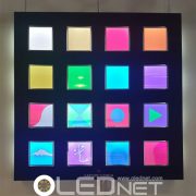
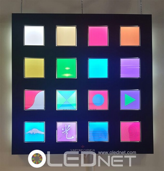
Sumitomo Chemical’s Decorative P-LED Lighting Panel, Lighting Japan 2016
Sumitomo Chemical revealed that they are planning to enter the general lighting market with solution process applied P-LED (polymer OLED).
Sumitomo Chemical is a company developing polymer and solution process applied OLED lighting panel. The company began actively selling decorative OLED lighting panel from H2 2015.
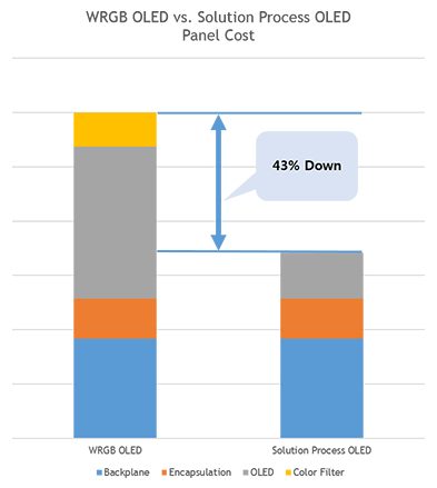
In Lighting Japan 2016 exhibition, Sumitomo Chemical announced that through their polymer materials and process technology, 80-90% of evaporation materials efficiency, and lifetime of approximately 20,000 hours at white 60-80 lm/w have been achieved. From 2017, they are planning to commercialize solution process OLED lighting panel as general lighting, as well as for decorative use, and revealed that the biggest issues are cost and improvement of consumers’ OLED awareness.
According to these issues, Sumitomo Chemical explained that although the cost of emitting area formed through solution process, cost down of evaporation formed emitting area and electrode part is required further. Although the 20,000 hours of lifetime is satisfactory, as consumers are aware that LED lighting’s lifetime is 40,000 hours or longer, Sumitomo Chemical pointed out it is important to change consumer’s OLED lighting awareness and understanding of lighting products.
by Moojong Lim, reporter@olednet.com