A seminar where latest technology of next generation display, OLED (Organic Light Emitting Diode), can be easily understood will take place. UBI Research, a research company specializing in OLED (http://www.ubiresearch.co.kr, president: Dr. Choong Hoon Yii), revealed that it will hold 2015 OLED Key Technology Seminar in COEX (Samseong-dong, Gangnam-gu, Seoul, South Korea) on 27 Aug.
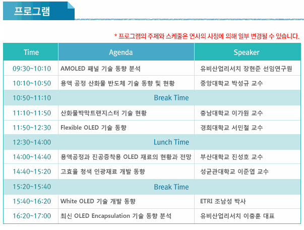
This seminar will discuss latest issues in OLED industry such as processes in flexible OLED, encapsulation, oxide-TFT, blue phosphorous emitting material, and solution process, and focus on technology development and its future.
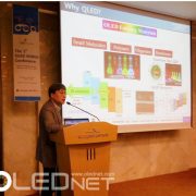
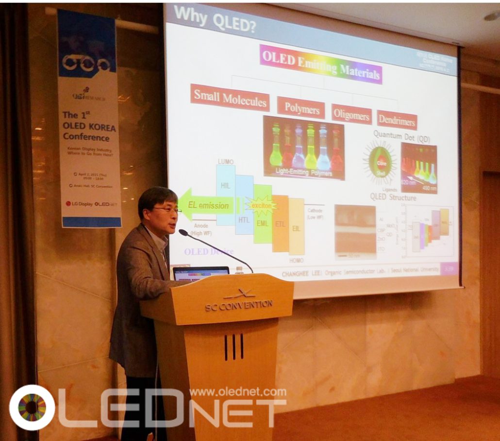
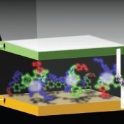
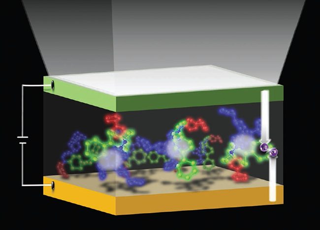
Encapsulation, which decides OLED panel’s final yield and lifetime, is an important process that determines exterior design in flexible OLED and large size OLED panel. It is also sensitive to light characteristics in surface light structure. At the 2015 OLED Key Technology Seminar, Dr. Choong Hoon Yi (president of UBI Research) is scheduled to introduce, through process and material analysis, essential technology needed for OLED panel to continue its growth and encapsulation technology trends.
At this seminar, Dr. Nam Sung Cho of ETRI (Electronics and Telecommunications Research Institute) will give a presentation on display technology that utilizes white OLED technology that is receiving much interest by Korean display market. He will detail white OLED technology’s present and future from lighting to large size TV.
Professor Sung Kyu Park of Chung-Ang University, will introduce oxide material that is in spotlight as display and next generation wearable device. He will also talk about internationally much discussed related technology trends and future progress.
Further presentation topics by OLED top experts include:
– AMOLED panel technology trends analysis (Hyun Jun Jang, senior researcher of UBI Research)
– Oxide-TFT technology status (Professor Ga-Won Lee, Chungnam National University)
– Solution process and vacuum evaporation OLED material’s status and forecast (Professor Sung-Ho Jin, Pusan National University)
– High efficiency blue phosphorous emitting material development trend (Professor Jun Yeob Lee, Sungkyunkwan University)
– Flexible OLED technology trend
UBI Research holds OLED Key Technology Seminars every year from 2011 and provides place for networking and sharing of information. Seminar registration can be completed through UBI Research website (www.ubiresearch.co.kr).

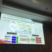
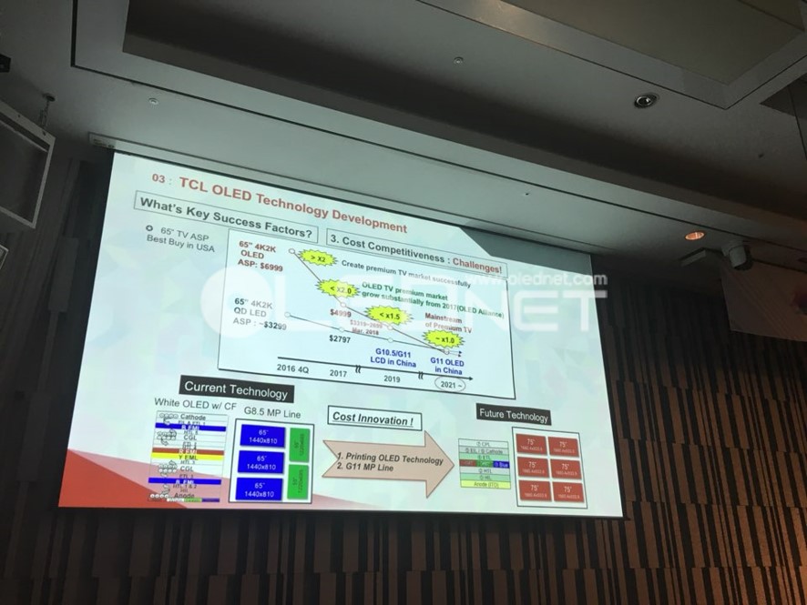
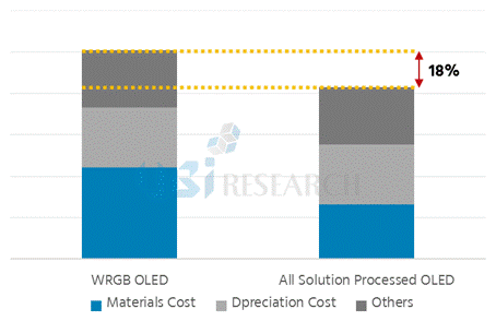
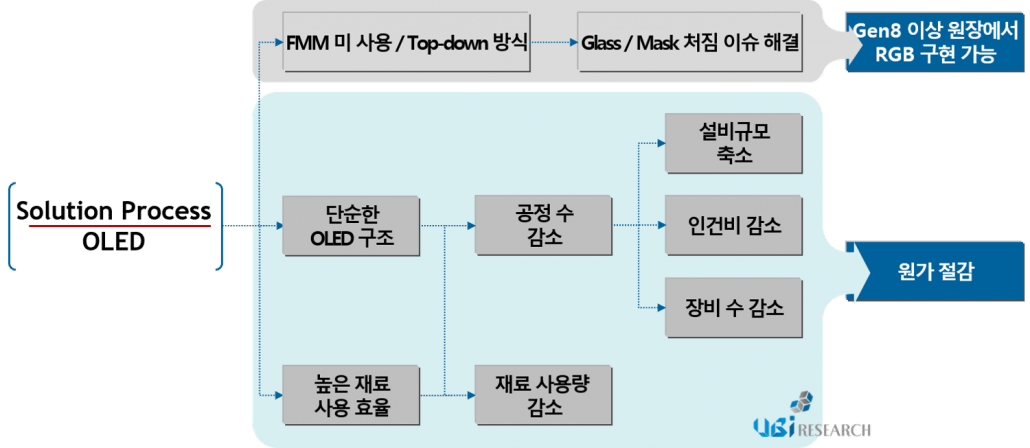
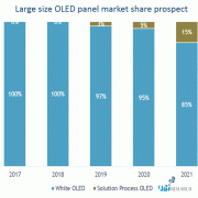
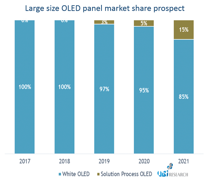
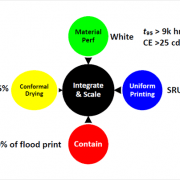
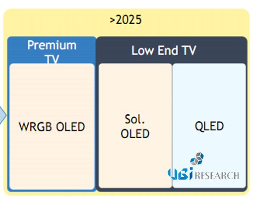
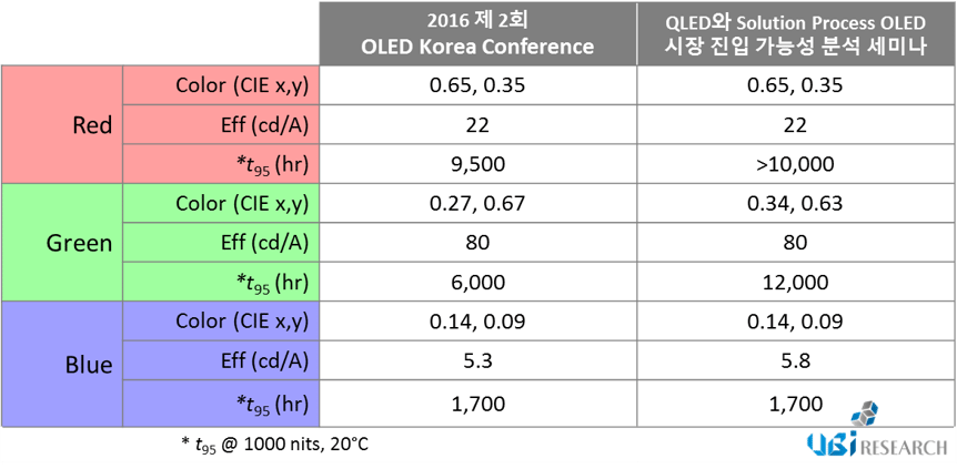
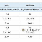
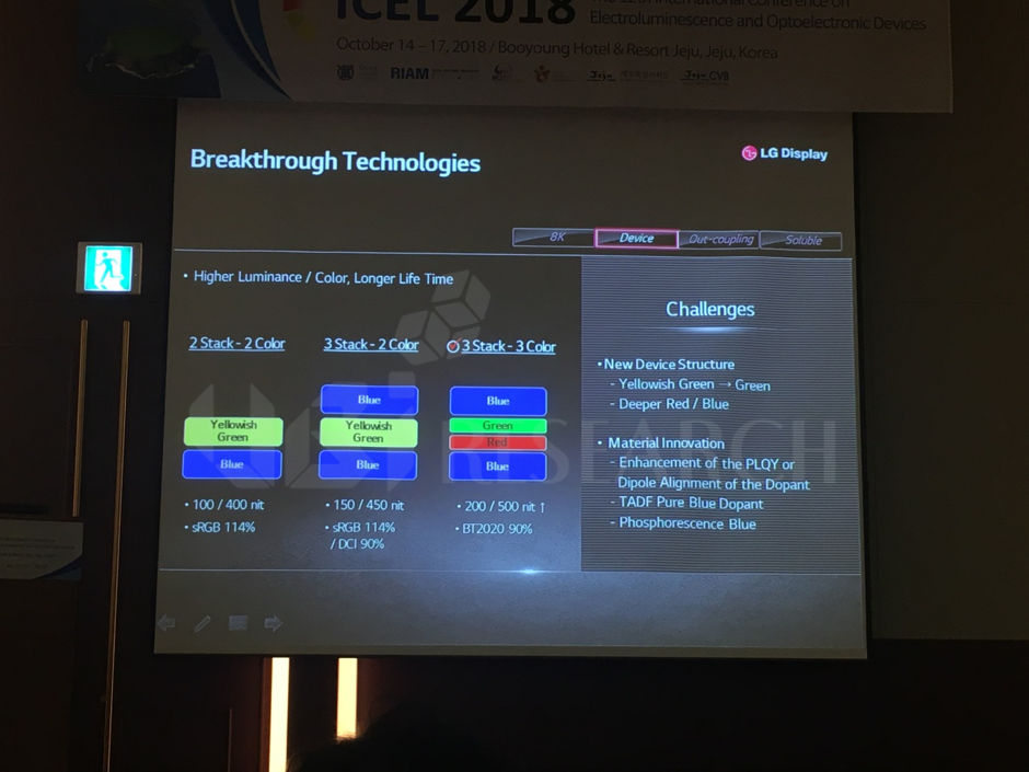 또한, LCD TV 가격에 대응하기 위한 기술로 solution process OLED를 언급하며 잉크젯 장비와 공정, soluble 재료의 개발도 필요하다고 밝혔다. 이를 위해서는 잉크젯 장비 개발과 대량 생산을 위한 공정 시간 단축도 필요하지만, soluble 재료의 성능과 신뢰성이 무엇보다도 중요할 것이라 언급했다.
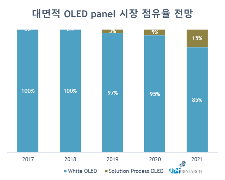
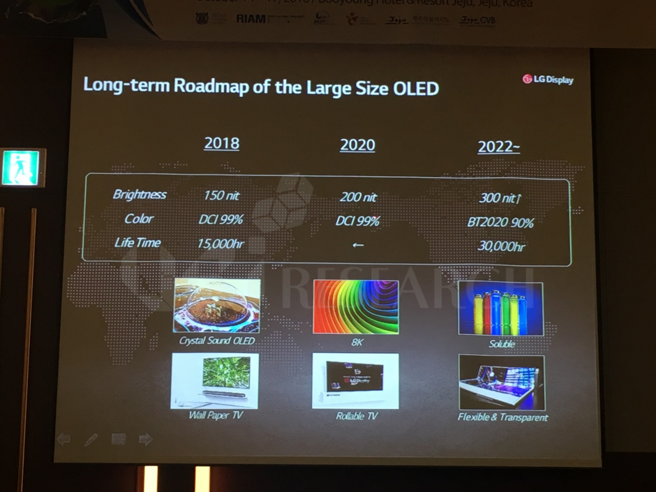


 .
.