Solution Process Panel, Cheaper To Produce than LCD

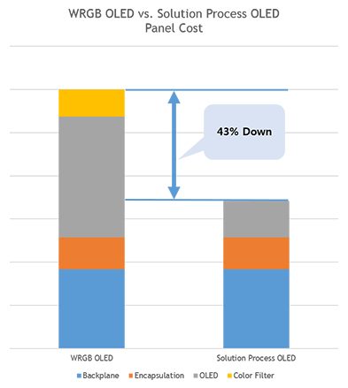
According to 2015 Solution Process OLED Report, published by UBI Research on October 14, solution process technology could produce 55inch OLED panel at approximately 43% cheaper cost compared to WRGB method.


The report added that this value is the result of analysis of 2015 Q2 55inch UHD OLED panel price and yield, which is slightly higher than current production price of 55inch UHD LCD panel. However, considering that the solution process OLED structure will become simplified and that yield of backplane and encapsulation can be improved, the OLED panels will be able to be produced at lower cost than LCD panel. The report also revealed that solution process OLED can be an alternative solution for large area OLED panel in achieving price competitiveness.


Solution process is a technology that can produce large area RGB pixel OLED panel using Gen8, or higher, equipment without cutting the mother glass. Key AMOLED panel companies are active in developing this technology.


However, as solvent is used in order to turn the existing evaporation material into ink, its purity is decreased leading to lower emitting efficiency and therefore lower lifetime. Despite these factors, key panel companies’ enthusiasm for solution process technology is due to the high emitting material usage efficiency without using color filter, and simple structure compared to WRGB OLED panel which leads to production cost decrease.


Panasonic has been most active in developing solution process applied OLED panel, and has presented several times in CES and IFA. BOE and AUO also have revealed solution process OLED panel produced via ink-jet manufacturing equipment, and CSOT is considering solution process development. Samsung Display and LG Display, leaders of AMOLED industry, are also actively developing the technology. LG Display has adopted Gen8 ink-jet manufacturing equipment, and Samsung Display has started solution process OLED panel development with a focus on ink-jet manufacturing equipment companies.


Material and manufacturing equipment companies as well as panel companies are leading the solution process technology development and commercialization. Kateeva agreed on technology collaboration with Sumitomo Chem. while Merck did the same with Seiko Epson. DuPont recently revealed that they enlarged solution process OLED material production facilities and began operation.


Following these participation by key panel, material, and manufacturing equipment companies in solution process technology development and commercialization, it is anticipated that the solution process OLED panel market will record rapid growth.


UBI Research’s 2015 Solution Process OLED Report forecast that solution process OLED panel market will actively begin mass production from 2018 and show approximately US$ 2,329 million in 2020.


Solution process OLED panel수정2

Solution process OLED panel, LCD보다 저렴하게 제작 가능

유비산업리서치에서 14일 발간한 “2015 Solution Process OLED Report”에 따르면 “Solution process로 55inch OLED panel을 현재 양산되고 있는 WRGB 방식의 OLED panel보다 약 43% 저렴하게 제작할 수 있다.”라고 분석했다.

보고서에서는 “2015년도 2사분기 기준 55inch UHD OLED panel 가격과 수율을 기준으로 분석한 수치로서 현재 55inch UHD LCD panel의 제조 원가보다는 약간 높게 나타났다. 하지만 solution process OLED의 구조가 단순화 될 것이라는 점과 backplane과 encapsulation 수율이 개선될 수 있는 점을 고려해보면 LCD panel보다 저렴하게 제조할 수 있을 것”이라고 덧붙이며 solution process OLED가 대면적 OLED panel의 가격경쟁력을 확보할 수 있는 대안이 될 것이라고 밝혔다.

Solution process는 대면적 OLED panel을 Gen8 이상의 장비에서 원장 분할 없이 RGB pixel 구조로 제조할 수 있는 기술이며 주요 AMOLED panel 업체에서 적극적으로 개발을 진행 중에 있다.

하지만 solution process에 적용되는 발광재료는 기존 증착재료를 ink화를 시키기 위해 solvent를 섞기 때문에 증착재료보다 순도가 낮아 발광효율이 떨어지고 수명이 낮을 수 밖에 없다. 그럼에도 불구하고 solution process를 주요 panel 업체들에서 적극적으로 개발하고 있는 이유는 color filter를 사용하지 않고 발광재료 사용효율이 높으며 WRGB방식의 OLED panel에 비해 구조가 단순하기 때문에 원가절감을 할 수 있다는 점이다.

Solution process를 적용한 OLED panel은 Panasonic에서 가장 적극적으로 개발을 진행해왔으며 CES와 IFA에서 여러 차례 공개한 적이 있다. BOE와 AUO도 ink-jet 장비를 이용한 solution process OLED panel을 공개한 바 있으며 CSOT에서도 기술개발 방향을 solution process로 검토 중에 있다. AMOLED 산업의 선두주자인 Samsung Display와 LG Display에서도 적극적으로 개발을 진행 중이다. LG Display는 Gen8 ink-jet 장비를 도입하였으며 Samsung Display도 ink-jet 장비업체들을 중심으로 solution process OLED panel 개발에 본격적으로 착수한 상태이다.

Panel 업체뿐만 아니라 재료와 장비업체들도 solution process 기술개발과 상용화에 앞장서고 있다. Kateeva와 Sumitomo Chem., Merck와 Seiko Epson은 기술 협업을 맺었으며 DuPont는 soluble OLED 재료 생산시설 규모를 늘리고 가동을 시작했다고 최근 밝힌 바 있다.

이처럼 solution process 기술 개발과 상용화에 panel 업체뿐만 아니라 주요 재료, 장비업체들이 참여함에 따라 solution process OLED panel 시장은 빠른 시일 내에 성장할 것으로 기대된다.

“2015 Solution Process OLED Report”에서는 solution process OLED panel 시장이 2018년부터 본격적으로 양산되기 시작하여 2020년 약 US$ 2,329 million 규모로 성장할 것으로 전망했다.

If the 600ppi Soluble process OLED is to be possible?

As a company producing ink-jet equipment for the soluble process OLED, Seiko Epson has already developed the ink-jet head which could realize up to 360ppi by arranging the 180ppi nozzles in 2 rows. Given that the resolution of the evaporation method RGB OLED is still in the 260ppi as a real RGB, it is a significantly useful technology in the development of high-resolution display.

Seiko Epson developed the technology to maintain total amount of ink in a fixed rate per pixel with the ink volume control and multiple nozzles, and also holds the technology to apply emissive layer evenly on the entire surface of HTL by making the surface of HTL and the contact angle of separation equal. In addition, the productions of the bottom emission OLED as well as the top emission OLED were succeeded in ink-jet. Top emission is possible when the HIL thin layer is applied extremely evenly using special combination of ink as the thickness of HIL layer influences greatly on the optical character.

Seiko Epson is planning to develop the 600ppi ink-jet head that arranges the 400ppi nozzles in two rows in order to develop the equipment producing hyper-resolution soluble process OLED. It is anticipated if it is possible to manufacture a hyper-resolution OLED of 600ppi, it will be the moment to replace LCD in the mobile display area for it could easily resolve the greatest weakness of OLED which is high-resolution issue.

Portfolio Items